Where is the best inductor placement on a switch mode PCB?
“Switching regulators for voltage conversion use inductors to temporarily store energy. These inductors are often very large in size and must be located in the printed circuit board (PCB) layout of the switching regulator. This task is not difficult because the current through the Inductor may change, but not instantaneously. Change can only be continuous, usually relatively slowly.
“
Throwing the question first: where should the coil be placed?
Switching regulators for voltage conversion use inductors to temporarily store energy. These inductors are often very large in size and must be located in the printed circuit board (PCB) layout of the switching regulator. This task is not difficult because the current through the Inductor may change, but not instantaneously. Change can only be continuous, usually relatively slowly.
A switching regulator switches current back and forth between two different paths. This switching is very fast, depending on the duration of the switching edge. The traces through which the switching current flows are called hot loops or AC current paths, which conduct current in one switching state and do not conduct current in the other switching state. In the PCB layout, the hot loop area should be kept small and the paths short in order to minimize the parasitic inductance in these traces. Parasitic trace inductance can create unwanted voltage offsets and cause electromagnetic interference (EMI).

Figure 1. Switching regulator for buck conversion (with critical hot loop shown as dashed line).
Figure 1 shows a buck regulator with the critical thermal loop shown as a dashed line. It can be seen that coil L1 is not part of the thermal loop. Therefore, it can be assumed that the placement of this inductor does not matter. It is correct to have the inductor outside the hot loop – so in the first example, placement is secondary. However, some rules should be followed.
Sensitive control traces must not be routed under the inductor (either on the surface or under the PCB), in inner layers, or on the back of the PCB. Influenced by the current flow, the coil generates a magnetic field, which as a result affects the weak signal in the signal path. In switching regulators, a critical signal path is the feedback path, which connects the output voltage to the switching regulator IC or Resistor divider.
It should also be noted that the actual coil has both capacitive and inductive effects. The first coil winding is directly connected to the switching node of the buck switching regulator, as shown in Figure 1. As a result, the voltage change in the coil is as strong and rapid as the voltage at the switch node. Due to the very short switching times and high input voltages in the circuit, considerable coupling effects occur on other paths on the PCB. Therefore, sensitive traces should be kept away from the coil.
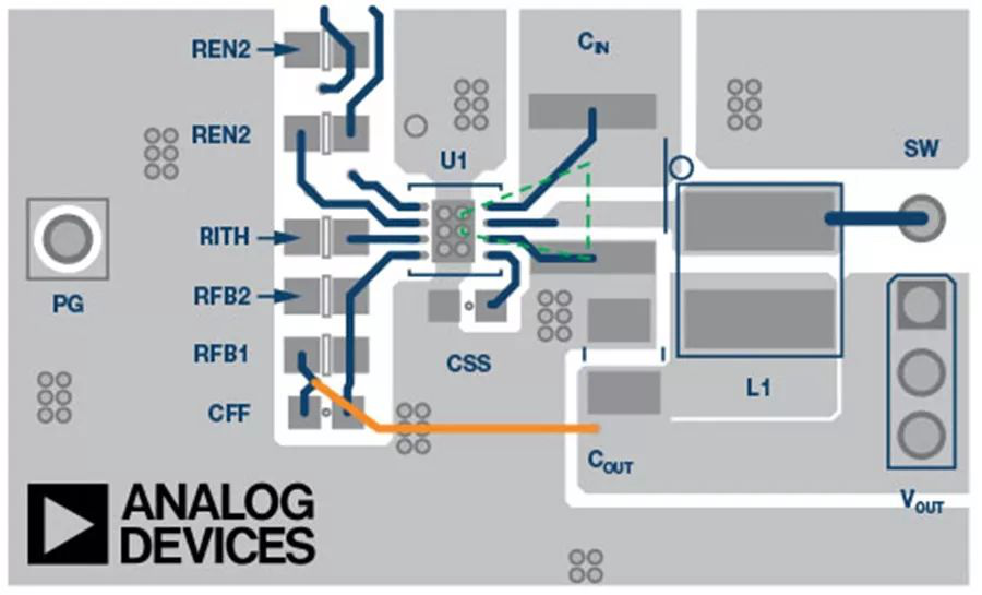
Figure 2. Example circuit of the ADP2360 buck converter with coil placement.
Figure 2 shows an example layout for the ADP2360. In this figure, the important thermal loops in Figure 1 are marked in green. As can be seen from the figure, the yellow feedback path is some distance away from the coil L1. It is on the inner layer of the PCB.
Some circuit designers don’t even want any copper layers in the PCB under the coil. For example, they provide cutouts under the inductor, even in the ground plane layer. The goal is to prevent the formation of eddy currents in the ground plane below the coil due to the coil magnetic field. There is nothing wrong with this approach, but there is also an argument that the ground plane should be consistent and not interrupted:
The ground plane used for shielding works best when it is not interrupted.
The more copper the PCB has, the better the heat dissipation.
Even if eddy currents occur, these currents can only flow locally, cause very little loss, and have little effect on the functionality of the ground plane.
So agree that the ground plane layer, even below the coil, should remain intact.
The Links: NL2432HC22-22A LTD104C11U